|
Monolayer Graphene on SiO2 Si 300 nm
Product Details:
- Color Transparent
- Material GRAPHENE FILM
- Application Graphene on SiO2,/Si
- Chemical Composition Graphene
10500 INR/Piece
X
Monolayer Graphene on SiO2 Si 300 nm Price And Quantity
- 10500 INR/Piece
- 1 Piece
Monolayer Graphene on SiO2 Si 300 nm Product Specifications
- Graphene on SiO2,/Si
- Graphene
- Transparent
- GRAPHENE FILM
Monolayer Graphene on SiO2 Si 300 nm Trade Information
- Paypal
- 20 Days
- Seal Packing
- North America Eastern Europe Middle East Asia
- All India
- Technical Data sheets are available upon request
Product Description
GRAPHENE FILM:
- Growth method: CVD synthesis
- Appearance (color): Transparent
- Transparency: > 97%
- Coverage: > 95%
- Number of graphene layers: 1
- Thickness (theoretical): 0.345 nm
- FET Electron Mobility on Al2O3 passivated SiO2/Si: 6900 cm2
- FET Electron Mobility on SiO2/Si: 3760 cm2
- Grain size: Up to 20 Um
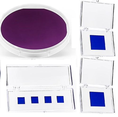
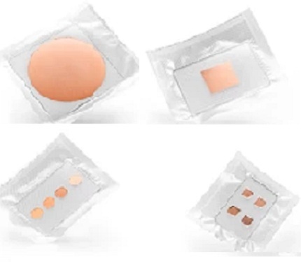
Available Sizes:
4" Wafer
10 mm x 10 mm -Pack of 4
10 mm x 10 mm
1 inch x 1 inch
Enter Buying Requirement Details
Other Products in 'CVD Films' category
Address
- B- 205, Prime Blue Forest, Rajapallya, Hoodi,Bengaluru - 560048, Karnataka, India
- Send Inquiry

 |
ULTRANANOTECH PRIVATE LIMITED
All Rights Reserved.(Terms of Use) Developed and Managed by Infocom Network Private Limited. |