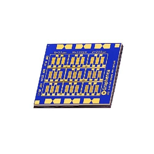
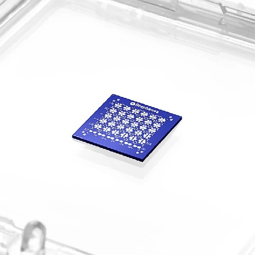
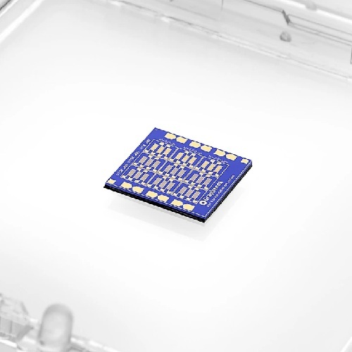
GFET-S12 (Die size 10 mm x 10 mm) - Processed in Clean Room Class 1000
The GFET-S12 chip from Graphenea provides 27 graphene devices distributed in a grid pattern on the chip. The devices have interdigitated contacts on top of the graphene channel, which are optimal for sensing of gases and volatile compounds. All the devices have the same channel length (1mm), but 3 different widths (50m, 100m and 200m). The interdigitated contacts have 3 different gaps (8m, 15m and 25m). These different graphene channel dimensions allow investigation of geometry dependence on device properties, enabling immediate device optimization.
TYPICAL SPECIFICATIONS
Growth method: CVD synthesis
Chip dimensions: 10 mm x 10 mm
Chip thickness: 675 m
Number of GFETs per chip: 27
Gate oxide thickness: 90 nm
Gate oxide material: SiO2
Dielectric Constant of the SiO2 layer: 3.9
Resistivity of substrate: 1-10 .cm
Metallization: Chromium/Gold 5/45nm
Graphene field-effect mobility: >1000 cm2/V.s
Dirac point: <50 V
Minimum working devices: >75 %
ABSOLUTE MAXIMUM RATINGS
Maximum gate-source voltage: 50 V
Maximum temperature rating: 150 C
Maximum drain-source current density 107A.cm-2
![]() |
ULTRANANOTECH PRIVATE LIMITED
All Rights Reserved.(Terms of Use) Developed and Managed by Infocom Network Private Limited. |