|

 Send Inquiry
8 inch Silicon Wafer
Price 15680.0 INR/ Piece
MOQ : 1 Number
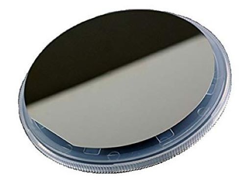
8 inch Silicon Wafer Specification
- Product Name
- Silicon wafer
- Product Type
- Silicon Wafers
- Color
- white
- Application
- Semiconductor device fabrication, MEMS, power electronics, R&D, and wafer processing studies.
- Shape
- circle
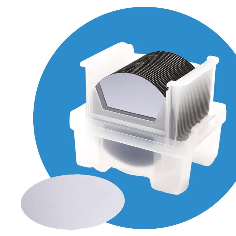
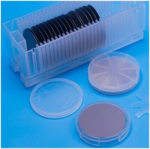
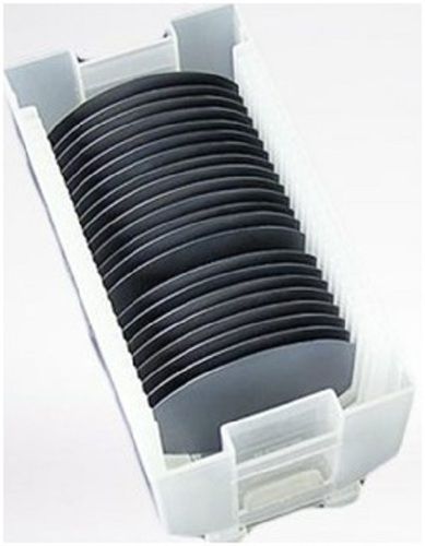
8 inch Silicon Wafer Trade Information
- Minimum Order Quantity
- 1 Number
- Payment Terms
- Paypal
- Supply Ability
- 10 Per Day
- Delivery Time
- 3 Days
- Packaging Details
- seal pack
- Main Export Market(s)
- Asia
About 8 inch Silicon Wafer
P-type (Boron Doped)
Dia: 8 inch (200 mm)
Orientation: 1 0 0
Thickness: 725 micron
Resistivity: 1- 20 ohm
Single side polished
A silicon wafer is a thin, flat slice of crystalline silicon that serves as the foundational substrate for the fabrication of semiconductor devices. Silicon wafers are the backbone of modern electronics and are used extensively in integrated circuits (ICs), microprocessors, memory chips, sensors, and photovoltaic devices. Due to silicons excellent electrical properties, thermal stability, and abundance, it has become the most widely used semiconductor material in the world.
Silicon wafers are manufactured with extremely high purity and precise crystal orientation to ensure reliable electrical performance. They form the starting material upon which complex electronic circuits are built through processes such as doping, oxidation, photolithography, and etching.
Material Properties of Silicon Wafer
The popularity of silicon wafers is attributed to their superior physical, electrical, and chemical properties. High-purity silicon crystals are grown using methods such as the Czochralski (CZ) process or the Float Zone (FZ) process.
Key properties include:
Excellent semiconducting behavior with controllable conductivity
High thermal conductivity for effective heat dissipation
Strong mechanical strength and dimensional stability
Ability to form a high-quality native oxide (SiO)
Chemical compatibility with standard semiconductor processing techniques
Silicon wafers are available in various diameters such as 2-inch, 4-inch, 6-inch, 8-inch, and 12-inch, with thickness carefully controlled to meet device fabrication requirements.
Types of Silicon Wafers
1. Based on Conductivity Type
Silicon wafers are classified as P-type or N-type depending on the dopant used. P-type wafers are doped with elements such as boron, while N-type wafers are doped with phosphorus, arsenic, or antimony. The conductivity type directly influences the electrical behavior of semiconductor devices.
2. Based on Crystal Structure
Most silicon wafers are single-crystal (monocrystalline), offering uniform electrical properties across the entire wafer. Polycrystalline silicon wafers are also used, especially in solar cell applications where cost efficiency is important.
3. Based on Surface Finish
Silicon wafers are supplied with different surface finishes, including single-side polished (SSP), double-side polished (DSP), and unpolished wafers. Polished wafers are essential for advanced microfabrication processes that require smooth and defect-free surfaces.
Applications of Silicon Wafer
1. Semiconductor and Integrated Circuits
Silicon wafers are the core material used in the manufacture of integrated circuits, microprocessors, logic devices, and memory chips. Almost all electronic devices, including computers, smartphones, and communication systems, rely on silicon-based ICs.
2. MEMS and Sensors
Silicon wafers are widely used in Micro-Electro-Mechanical Systems (MEMS) such as pressure sensors, accelerometers, gyroscopes, and microphones. The mechanical strength and process compatibility of silicon make it ideal for precise micro-scale structures.
3. Solar Cells and Photovoltaics
In the renewable energy sector, silicon wafers are used to manufacture crystalline solar cells. Both monocrystalline and polycrystalline silicon wafers convert sunlight into electricity with high efficiency and long-term stability.
4. Power Electronics
Silicon wafers are used in power devices such as diodes, transistors, MOSFETs, and IGBTs. These devices are essential for power management in electric vehicles, industrial drives, power supplies, and renewable energy systems.
5. Research and Development
Silicon wafers are extensively used in academic and industrial research laboratories for material studies, thin film deposition, device prototyping, and semiconductor process development.
Tell us about your requirement

Price:
Quantity
Select Unit
- 50
- 100
- 200
- 250
- 500
- 1000+
Additional detail
Mobile number
Email

More Products in Silicon Wafer Category
2 inch Intrinsic Silicon Wafer
Price 2500.0 INR / Piece
Minimum Order Quantity : 1 Piece
Shape : Circular
Material : Single Crystal
Product Name : Silicon Wafer Intrinsic: Diameter2 inch
Color : Shinning grey
3inch P Type Silicon Wafer
Price 2900.0 INR / Piece
Minimum Order Quantity : 1 Piece
Shape : Circular
Material : Single Crystal
Product Name : Silicon Wafer P Type: Diameter3 inch
Color : Shinning grey
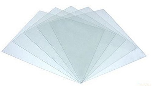
ITO Coated Glass
Price 1500 INR / Piece
Minimum Order Quantity : 1 Piece
Shape : Rectangle
Material : ITO
Product Name : ITO Coated Glass
Color : Transparent
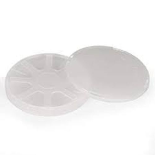
silicon wafer carrier box 3 inch
Price 3186.0 INR / Piece
Minimum Order Quantity : 3 Pieces
Shape : Circular
Material : polypropylene
Product Name : Carrier box
Color : White
Address
GST : 29AABCU9740P1ZH
- B- 205, Prime Blue Forest, Rajapallya, Hoodi,Bengaluru - 560048, Karnataka, India
- Phone :08071930855
- Send Inquiry
 |
ULTRANANOTECH PRIVATE LIMITED
All Rights Reserved.(Terms of Use) Developed and Managed by Infocom Network Private Limited. |
