|

 Send Inquiry
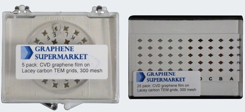
CVD Graphene on Transmission Electron Microscopy (TEM) Grids
Price 8500 INR/ Pack
MOQ : 1 Pack
CVD Graphene on Transmission Electron Microscopy (TEM) Grids Specification
- Usage
- Materials science and Semiconductor Research
- Material
- CVD Graphene TEM grids
- Application
- grids
- Chemical Composition
- Graphene
- Product Type
- TEM grids
CVD Graphene on Transmission Electron Microscopy (TEM) Grids Trade Information
- Minimum Order Quantity
- 1 Pack
- Payment Terms
- Paypal
- Delivery Time
- 20 Days
- Packaging Details
- seal packing
- Main Export Market(s)
- North America, Eastern Europe, Middle East, Asia
- Main Domestic Market
- All India
- Certifications
- Technical Data sheets are available upon request
About CVD Graphene on Transmission Electron Microscopy (TEM) Grids
We use CVD graphene grown on Ni to prepare TEM grids
Thickness of CVD Graphene film: 0.3-2 nm (1-6 monolayers)
Typical graphene coverage:60-90%
Ultrathin CVD Graphene grids provide the ideal specimen support to achieve high resolution data in TEM imaging making them an ideal choice many TEM applications such as:
CVD Graphene grids can be used for the applications:
- Imaging of nanoparticles, proteins, viruses, DNA
- Medical Diagnostics
- Single Cell Studies
- 3D protein imaging
- Drug design
- Imaging of Biological Markers and bio-inspired nanomaterials
- Cryo-transmission electron microscopy, Electron Cryomicroscopy
- Single Particle Analysis ( SPA )
- Materials science and Semiconductor Researc
- Electron Energy Loss Spectroscopy (EELS)
Available Size:
- 5 pack
- 25 pack
- Trial pack 10 CVD Graphene TEM Grids
Tell us about your requirement

Price:
Quantity
Select Unit
- 50
- 100
- 200
- 250
- 500
- 1000+
Additional detail
Mobile number
Email

More Products in CVD Films Category
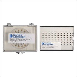
Graphene on Copper 2000 TEM Grids
Price 12000 INR / Piece
Minimum Order Quantity : 1 , , Piece
Application : Graphene on Copper
Material : CVD graphene
Chemical Composition : Graphene
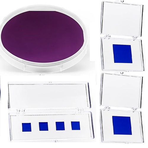
Monolayer Graphene on SiO2 Si 300 nm
Price 10500 INR / Piece
Minimum Order Quantity : 1 Piece
Application : Graphene on SiO2,/Si
Material : GRAPHENE FILM
Color : Transparent
Chemical Composition : Graphene
Monolayer Graphene on Cu
Price 10000 INR / Piece
Minimum Order Quantity : 1 Piece
Application : Graphene on Copper
Material : GRAPHENE FILM
Color : Transparent

Monolayer Graphene on Cu with PMMA Coating
Price 20000.0 INR / Piece
Minimum Order Quantity : 1 Piece
Application : Graphene on Copper
Material : Monolayer Graphene
Color : Transparent
Chemical Composition : Graphene
Address
GST : 29AABCU9740P1ZH
- B- 205, Prime Blue Forest, Rajapallya, Hoodi,Bengaluru - 560048, Karnataka, India
- Phone :08071930855
- Send Inquiry
 |
ULTRANANOTECH PRIVATE LIMITED
All Rights Reserved.(Terms of Use) Developed and Managed by Infocom Network Private Limited. |
