|

 Send Inquiry
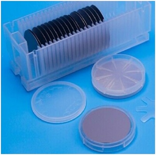
Industrial Silicon Wafer Diameter Intrinsic (4-inch)
Price 4000 INR/ Piece
MOQ : 1 Piece
Industrial Silicon Wafer Diameter Intrinsic (4-inch) Specification
- Product Name
- Silicon Wafer Diameter Intrinsic (4-inch)
- Product Type
- Wafer
- Material
- Silicon
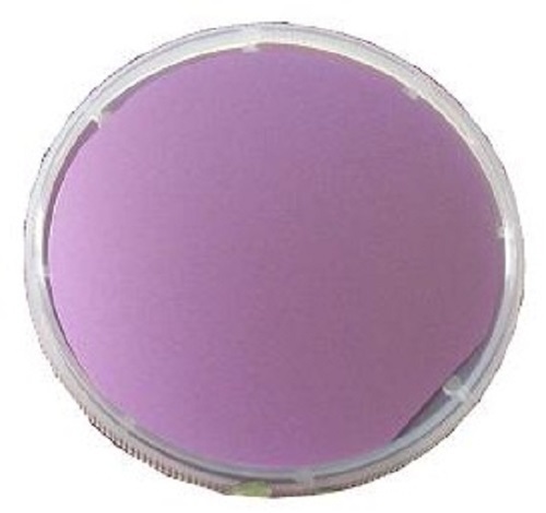
- Color
- Grey
- Application
- Semiconductor, Solar Cells, Research and Development
- Shape
- Round
- Density
- 2.33 Gram per cubic centimeter(g/cm3)
- Hardness
- High
- Type
- Intrinsic (Undoped)
- Flatness (TTV)
- < 10 m
- Moisture Resistance
- High
- Impurity Level
- < 1 ppb metal contaminants
- Surface Finish
- Single Side Polished (SSP) or Double Side Polished (DSP)
- Edge Type
- Beveled Edge
- Operating Temperature
- Up to 1200C (inert atmosphere)
- Standard Packing
- Cassette or Vacuum-sealed box
- Diameter
- 4 inch (100 mm)
- Thickness
- 525 25 m
- Warp
- < 30 m
- Resistivity
- > 5000 cm (Intrinsic)
Industrial Silicon Wafer Diameter Intrinsic (4-inch) Trade Information
- Minimum Order Quantity
- 1 Piece
- Payment Terms
- Paypal
- Supply Ability
- 25 Pieces Per Day
- Delivery Time
- 5 Days
- Main Export Market(s)
- Middle East, Eastern Europe, Australia, Asia
- Main Domestic Market
- All India
About Industrial Silicon Wafer Diameter Intrinsic (4-inch)
Experience pivotal quality with the illustrious Silicon Wafer Diameter Intrinsic (4-inch), ideal for top-tier research and industrial applications. As a distributor, manufacturer, supplier, retailer, and trader in India, we offer unbeatable value - grab the opportunity to procure wafers featuring 4-inch (100 mm) diameter, high flatness, and minimal warp. With options for <100> or <111> orientations, ultra-low impurity levels (<1 ppb), exceptional moisture resistance, and a robust hardness, these products ensure reliability for semiconductor, solar cell, and R&D settings. Select single or double side polished finish. Secure your advanced solution today!
Versatile Usage Across Critical Applications
The Silicon Wafer Diameter Intrinsic (4-inch) serves as a pivotal element in semiconductor device fabrication, solar cell production, and advanced research. With its round, highly polished surface and undoped nature, it is optimally used for prototyping, critical device testing, and R&D in pioneering technologies. Its top-tier thermal and moisture resistance makes it the option of choice for laboratories, academic institutions, and leading electronics manufacturers seeking value in their work.
Certifications, Payment and Export Packaging
Our Silicon Wafer Diameter Intrinsic (4-inch) complies with stringent certifications suitable for the global export market. Flexible payment terms, including advance, LC, and quoted outlay per order, streamline procurement. Wafers are meticulously packed in cassettes or vacuum-sealed boxes to maintain integrity during export. Each shipment is supported with necessary documentation and specifications, ensuring you receive a quality-assured product at every stage, from quotation to delivery.
FAQ's of Silicon Wafer Diameter Intrinsic (4-inch):
Q: How is the Silicon Wafer Diameter Intrinsic (4-inch) typically used?
A: The wafer is primarily employed in semiconductor manufacturing, solar cell development, and various R&D projects requiring undoped, intrinsic silicon substrates with high resistivity and low impurity.Q: What are the options for crystal orientation and surface finish on these wafers?
A: Customers can specify crystal orientation as <100> or <111>, and choose between single side polished (SSP) or double side polished (DSP) surface finish based on their application requirements.Q: Where does this product find its most pivotal applications?
A: These wafers are commonly found in advanced electronics industries, universities, and research institutes involved in developing or testing semiconductor devices and solar technologies.Q: What is the process for procuring a quotation and placing an order?
A: To get a quotation, simply contact us with your required specifications. We will provide a clear outlay and payment options. Once confirmed, your order is processed for swift dispatch.Q: What makes this wafer a top-tier choice for research and development purposes?
A: Its high purity, minimal metal contamination, and superior flatness offer unmatched consistency and reliability, making it invaluable for critical experimentation and device prototyping.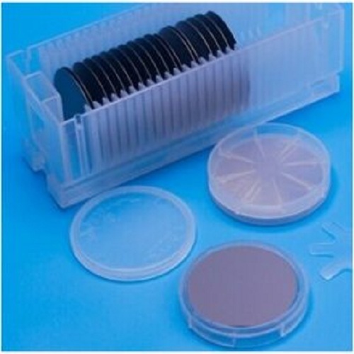
Tell us about your requirement

Price:
Quantity
Select Unit
- 50
- 100
- 200
- 250
- 500
- 1000+
Additional detail
Mobile number
Email

More Products in Silicon Wafer Category
2inch Silicon Wafer Intrinsic
Price 2000 INR / Piece
Minimum Order Quantity : 1 Piece
Product Name : Silicon Wafer Intrinsic : Diameter2 inch
Material : Single Crystal
Product Type : Undoped/Intrinsic
Shape : Circular

4 Inch N Type Silicon And Silicon Oxide Wafer
Price 2300 INR / Piece
Minimum Order Quantity : 1 Piece
Product Name : Silicon / Silicon Oxide, Wafer N Type Diameter : 4 inch
Material : Single Crystal
Product Type : N Type
Shape : Circular
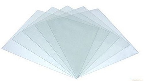
ITO Coated Glass
Price 1500 INR / Piece
Minimum Order Quantity : 1 Piece
Product Name : ITO Coated Glass
Material : ITO
Product Type : ITO
Shape : Rectangle
N Type Silicon Oxide Wafer
Price 6000 INR / Piece
Minimum Order Quantity : 1 Piece
Product Name : Silicon / Silicon Oxide, Wafer N Type Diameter : 4 inch
Material : Single Crystal
Product Type : N Type
Shape : Circular
Address
GST : 29AABCU9740P1ZH
- B- 205, Prime Blue Forest, Rajapallya, Hoodi,Bengaluru - 560048, Karnataka, India
- Phone :08071930855
- Send Inquiry
 |
ULTRANANOTECH PRIVATE LIMITED
All Rights Reserved.(Terms of Use) Developed and Managed by Infocom Network Private Limited. |
