|

 Send Inquiry
Molybdenum Disulfide (MoS2) Pristine
Price 17500 - 18000.00 INR/ Milliliter
MOQ : 100 Milliliters
Molybdenum Disulfide (MoS2) Pristine Specification
- Grade
- research grade
- Shape
- Other
- Size
- 100-400 nm
Molybdenum Disulfide (MoS2) Pristine Trade Information
- Minimum Order Quantity
- 100 Milliliters
- Supply Ability
- 1 Milliliter Per Day
- Delivery Time
- 15 Days
- Packaging Details
- cartons & wooden packing
- Main Export Market(s)
- Asia
- Main Domestic Market
- All India
About Molybdenum Disulfide (MoS2) Pristine
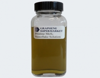
Molybdenum Disulfide (MoS2) Pristine Flakes in Solution 100 ml
Molybdenum Disulfide (MoS2) Pristine Flakes in Solution, 100 ML
MoS2 Pristine Flakes are nanoscale crystals dispersed in ethanol/water solution. If separated from the solution, nano-MoS2 forms emerald-green crystals that look different from the silver-black crystals of bulk MoS2.
SEM image of an Individual flake

UV-Visible Absorption Spectrum

Each Mo(IV) center of MoS2 is occupying a trigonal prismatic coordination sphere, which is bound to six sulfide ligands. The sulfur centre is connected to three Molybdenum centres, which are pyramidal. The trigonal prisms are layered, sandwiching molybdenum atoms between layers of sulfur atoms.
Depiction of MoS2 Crystal Structure1

MoS2 in its monolayer form has recently been under particular recognition for its intriguing electrical and optical properties. Bulk MoS2is generally an n-type semiconductor with an indirect bandgap (-1.3 eV) and a carrier mobility in the range of 50-200 cm2 V-1s-1 at room temperature. On the other hand, monolayer MoS2 has a direct bandgap of -1.8 eV, and can be useful in low-power switching devices.
MoS2 Raman Spectrum

AFM Image of an MoS2 Flake on SiO2

Preparation Method: Solution-Based Exfoliation
Applications:
- Transistors
- Flexible Displays
- Optics
- MoS2 Research
- Inks
- Thin Semiconducting Films
This solution can be easily deposited onto a substrate or surface of your choice to form a thin film coating.
SEM Image of an MoS2 Thin Film on SiO2


Key Features
- Lateral Size: 100-400 nm
- Thickness: 1-8 monolayers
- Purity in dry phase: >99%
- Solution Concentration: 18 mg/L
- Solution is stable under ambient conditions
Tell us about your requirement

Price:
Quantity
Select Unit
- 50
- 100
- 200
- 250
- 500
- 1000+
Additional detail
Mobile number
Email

More Products in Solutions Category
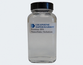
Boron Nitride (BN) Pristine Flakes in Solution 100
Price 17500.00 - 18000.00 INR / Millimeter
Minimum Order Quantity : 50 Milliliters
Size : 50200 nm
Weight : 0.10 Pound (lb)
Grade : research grade
Shape : Other
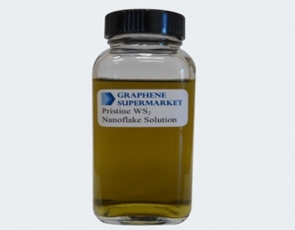
Tungsten Disulfide (WS2) Pristine Flakes
Price 17500.00 - 18000.00 INR / Millimeter
Minimum Order Quantity : 100 Milliliters
Size : 50150 nm
Weight : 0.10 Pound (lb)
Grade : research grade
Shape : Powder
Address
GST : 29AABCU9740P1ZH
- B- 205, Prime Blue Forest, Rajapallya, Hoodi,Bengaluru - 560048, Karnataka, India
- Phone :08071930855
- Send Inquiry
 |
ULTRANANOTECH PRIVATE LIMITED
All Rights Reserved.(Terms of Use) Developed and Managed by Infocom Network Private Limited. |
