|

 Send Inquiry
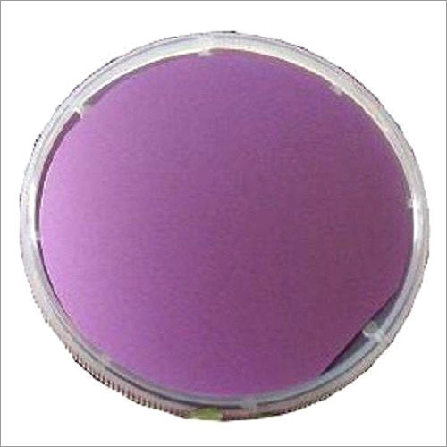
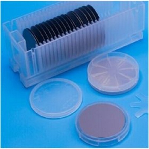
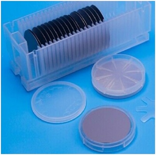
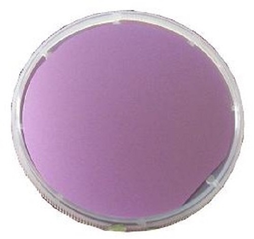
Silicon Oxide Wafer (P type)
Price 3500.0 INR/ Piece
MOQ : 1 Piece
Silicon Oxide Wafer (P type) Specification
- Product Name
- Silicon Oxide Wafer (P type)
- Material
- Silicon Wafer
- Color
- grey
- Application
- Semiconductor Devices,MEMS (Micro-Electro-Mechanical Systems),Advanced Electronics
- Shape
- Round
Silicon Oxide Wafer (P type) Trade Information
- Minimum Order Quantity
- 1 Piece
- Payment Terms
- Paypal
- Delivery Time
- 4 Days
- Main Export Market(s)
- Asia, North America, Eastern Europe, Middle East
- Main Domestic Market
- All India
About Silicon Oxide Wafer (P type)
- Silicon OxideWafer (P type)
- Diameter 100 mm 0.2 mm(4")
- Oxide Thickness:300 20 nm ( dry)
- Wafer thickness:500 20 micron
- Resistivity:1-10 ohm-cm
- Type/Dopant: P
- Orientation: 1 0 0
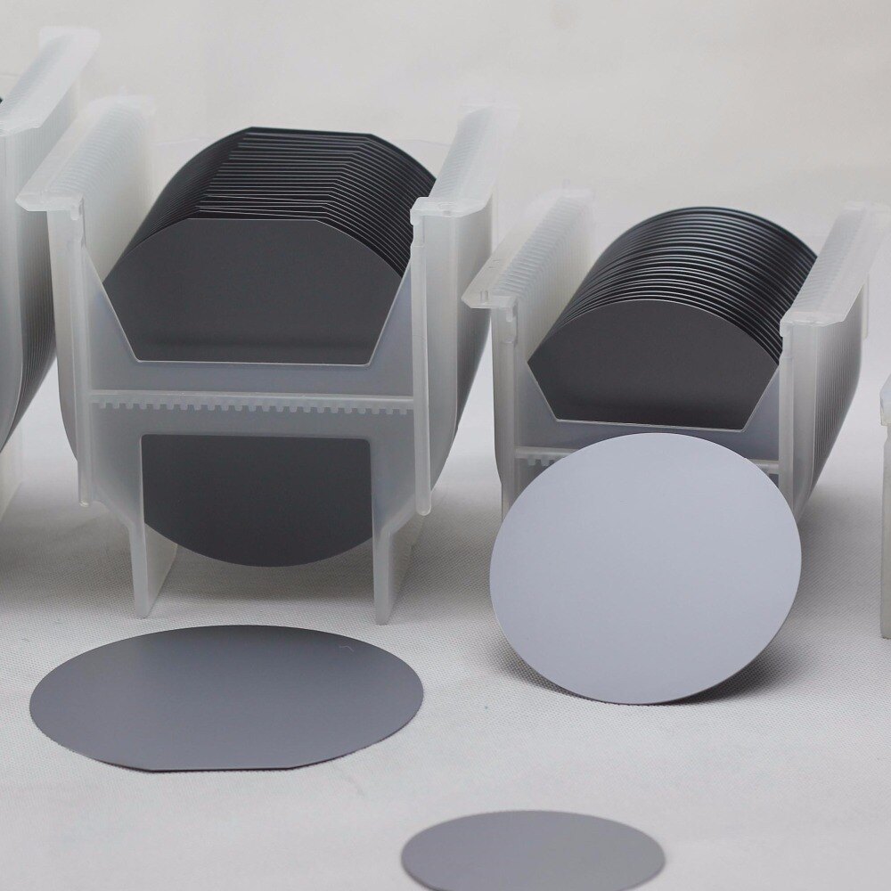
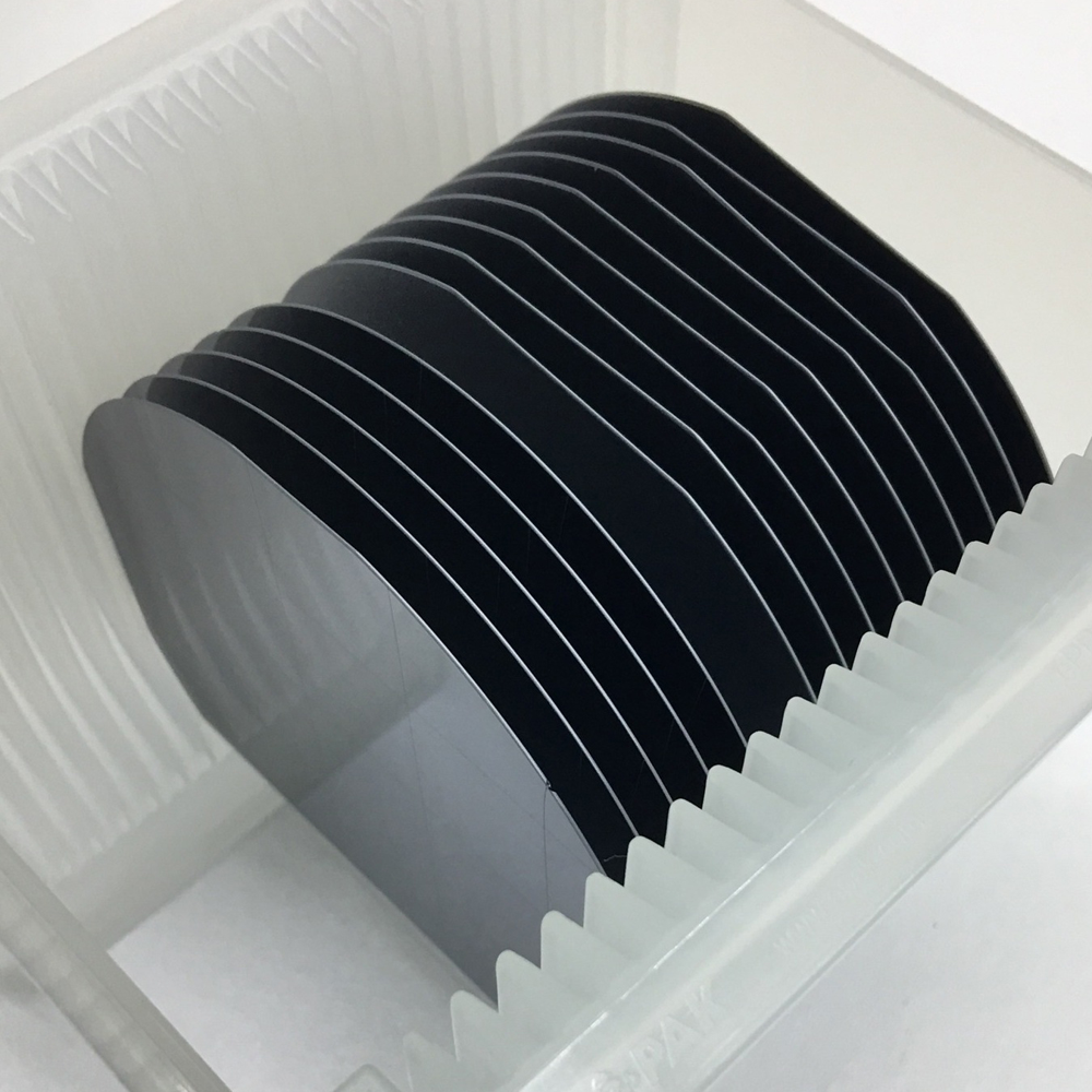
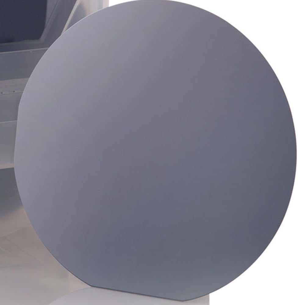
Silicon Oxide (SiO) Wafer
Introduction
Silicon oxide wafers, commonly known as SiO wafers, are widely used in semiconductor technology, microelectronics, MEMS (Micro-Electro-Mechanical Systems), and optoelectronics. Silicon oxide is an insulating material with excellent thermal stability, chemical resistance, and electrical insulation properties.
SiO wafers serve as substrates or insulating layers in various devices, providing mechanical support while maintaining electrical isolation between active layers. They are also used in research applications, sensors, and as dielectric layers in MOSFETs and IC fabrication.
The combination of high purity, smooth surfaces, and precise thickness control makes SiO wafers essential for high-performance electronic and microfabrication applications.
Material Properties of Silicon Oxide Wafer
Silicon oxide exhibits unique physical, electrical, and chemical characteristics that make it indispensable in semiconductor technology.
Key Properties:
- High electrical resistivity, making it an excellent insulator
- Thermal stability up to high processing temperatures (typically 1000C)
- Chemical resistance to acids, bases, and most solvents
- Smooth surface finish with minimal defects for photolithography processes
- Optical transparency in the visible and near-infrared range
Dimensions and Specifications:
- Standard diameters: 2-inch, 3-inch, 4-inch, 6-inch, 8-inch, 12-inch
- Thickness: 0.2 mm to 0.7 mm (can vary based on application)
- Surface finish: single-side polished (SSP) or double-side polished (DSP)
- Surface roughness: typically less than 1 nm RMS for high-precision applications
Types of Silicon Oxide Wafers
1. Thermal Oxide Wafers
Thermal oxidation is a process in which a silicon wafer is exposed to high temperatures in the presence of oxygen or steam to grow a silicon dioxide layer on its surface. These wafers are widely used in MOS devices, gate oxides, and capacitors.
2. CVD (Chemical Vapor Deposition) Oxide Wafers
CVD techniques are used to deposit silicon oxide layers on silicon wafers for insulation, passivation, or protective coating purposes. CVD oxide offers uniform thickness and conformal coverage over complex structures.
3. Fused Silica Wafers
Fused silica wafers are pure silicon dioxide wafers with extremely low defect densities and high optical transparency. They are used in optics, laser applications, and high-temperature processes.
4. Oxide-on-Silicon Wafers (SOI Structures)
Silicon-on-insulator (SOI) wafers consist of a thin silicon layer on top of an insulating silicon dioxide layer. These are used in high-performance microelectronics and MEMS devices to reduce parasitic capacitance and improve device speed.
Applications of Silicon Oxide Wafers
1. Semiconductor Devices
- Used as gate oxide layers in MOSFETs
- Insulating layers in IC fabrication
- Dielectric layers in capacitors and transistors
2. MEMS Devices
- Silicon oxide wafers provide mechanical support and insulation for microstructures such as sensors, actuators, and microfluidic devices.
- Commonly used in pressure sensors, accelerometers, and gyroscopes.
3. Optoelectronic and Photonic Applications
- Transparent SiO wafers are used in optical waveguides, laser substrates, and optical filters.
- Provides high transparency and low absorption in the visible and infrared range.
4. Research and Development
- SiO wafers are widely used in academic and industrial research laboratories.
- Ideal for thin-film deposition experiments, etching studies, and surface functionalization.
5. Solar Cells and Photovoltaics
- Used as dielectric or passivation layers in high-efficiency solar cells.
- Improves electrical performance and reduces recombination losses.
Advantages of Silicon Oxide Wafers
- High electrical insulation and resistivity
- Excellent thermal and chemical stability
- Smooth, defect-free surfaces for advanced microfabrication
- Compatible with standard semiconductor processing
- Available in various sizes and thicknesses to suit application needs
Limitations
- Brittle and fragile; requires careful handling
- Limited mechanical strength compared to silicon wafers
- Thermal expansion mismatch with some materials can cause stress in multilayer devices
- Not conductive; requires additional conductive layers for electronic applications
- Silicon OxideWafer (P type)
- Diameter 100 mm 0.2 mm(4")
- Oxide Thickness:300 20 nm ( dry)
- Wafer thickness:500 20 micron
- Resistivity:1-10 ohm-cm
- Type/Dopant: P
- Orientation: 1 0 0
Silicon Oxide (SiO) Wafer
Introduction
Silicon oxide wafers, commonly known as SiO wafers, are widely used in semiconductor technology, microelectronics, MEMS (Micro-Electro-Mechanical Systems), and optoelectronics. Silicon oxide is an insulating material with excellent thermal stability, chemical resistance, and electrical insulation properties.
SiO wafers serve as substrates or insulating layers in various devices, providing mechanical support while maintaining electrical isolation between active layers. They are also used in research applications, sensors, and as dielectric layers in MOSFETs and IC fabrication.
The combination of high purity, smooth surfaces, and precise thickness control makes SiO wafers essential for high-performance electronic and microfabrication applications.
Material Properties of Silicon Oxide Wafer
Silicon oxide exhibits unique physical, electrical, and chemical characteristics that make it indispensable in semiconductor technology.
Key Properties:
- High electrical resistivity, making it an excellent insulator
- Thermal stability up to high processing temperatures (typically 1000C)
- Chemical resistance to acids, bases, and most solvents
- Smooth surface finish with minimal defects for photolithography processes
- Optical transparency in the visible and near-infrared range
Dimensions and Specifications:
- Standard diameters: 2-inch, 3-inch, 4-inch, 6-inch, 8-inch, 12-inch
- Thickness: 0.2 mm to 0.7 mm (can vary based on application)
- Surface finish: single-side polished (SSP) or double-side polished (DSP)
- Surface roughness: typically less than 1 nm RMS for high-precision applications
Tell us about your requirement

Price:
Quantity
Select Unit
- 50
- 100
- 200
- 250
- 500
- 1000+
Additional detail
Mobile number
Email

More Products in Silicon Wafer Category
Industrial Silicon Wafer Diameter Intrinsic (4-inch)
Price 4000 INR / Piece
Minimum Order Quantity : 1 Piece
Material : Silicon
Product Name : Silicon Wafer Diameter Intrinsic (4inch)
Product Type : Wafer
Color : Grey
2inch Silicon Wafer Intrinsic
Price 2000 INR / Piece
Minimum Order Quantity : 1 Piece
Material : Single Crystal
Product Name : Silicon Wafer Intrinsic : Diameter2 inch
Product Type : Undoped/Intrinsic
Color : Shinning grey
N Type Silicon Oxide Wafer
Price 6000 INR / Piece
Minimum Order Quantity : 1 Piece
Material : Single Crystal
Product Name : Silicon / Silicon Oxide, Wafer N Type Diameter : 4 inch
Product Type : N Type
silicon wafer carrier box 3 inch
Price 3186.0 INR / Piece
Minimum Order Quantity : 3 Pieces
Material : polypropylene
Product Name : Carrier box
Product Type : Wafer
Color : White
Address
GST : 29AABCU9740P1ZH
- B- 205, Prime Blue Forest, Rajapallya, Hoodi,Bengaluru - 560048, Karnataka, India
- Phone :08071930855
- Send Inquiry
 |
ULTRANANOTECH PRIVATE LIMITED
All Rights Reserved.(Terms of Use) Developed and Managed by Infocom Network Private Limited. |
