|

 Send Inquiry
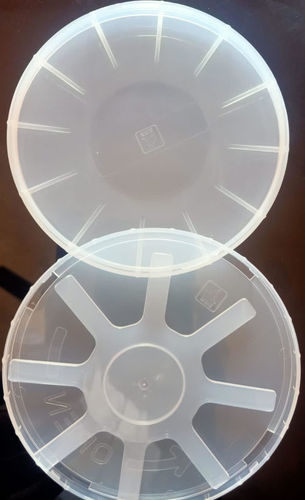
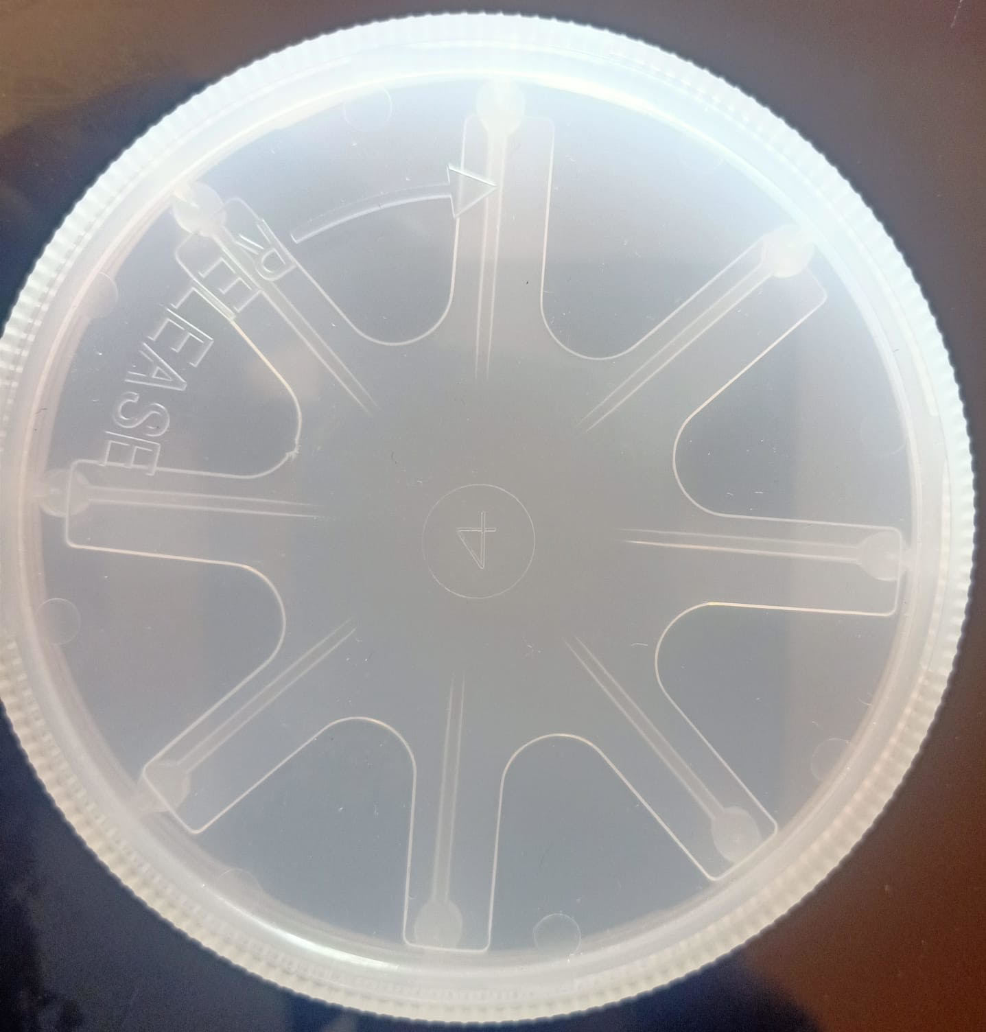
Silicon Wafer Carrier Box Polypropylene Material
Price 5000.0 INR/ Box
MOQ : 1 Box
Silicon Wafer Carrier Box Polypropylene Material Specification
- Product Name
- silicon wafer carrier box polypropylene material
- Product Type
- polypropylene
- Material
- polypropylene
- Color
- Transparent
- Shape
- Round
Silicon Wafer Carrier Box Polypropylene Material Trade Information
- Minimum Order Quantity
- 1 Box
- Delivery Time
- 20 Days
- Main Export Market(s)
- Asia
- Main Domestic Market
- All India
About Silicon Wafer Carrier Box Polypropylene Material
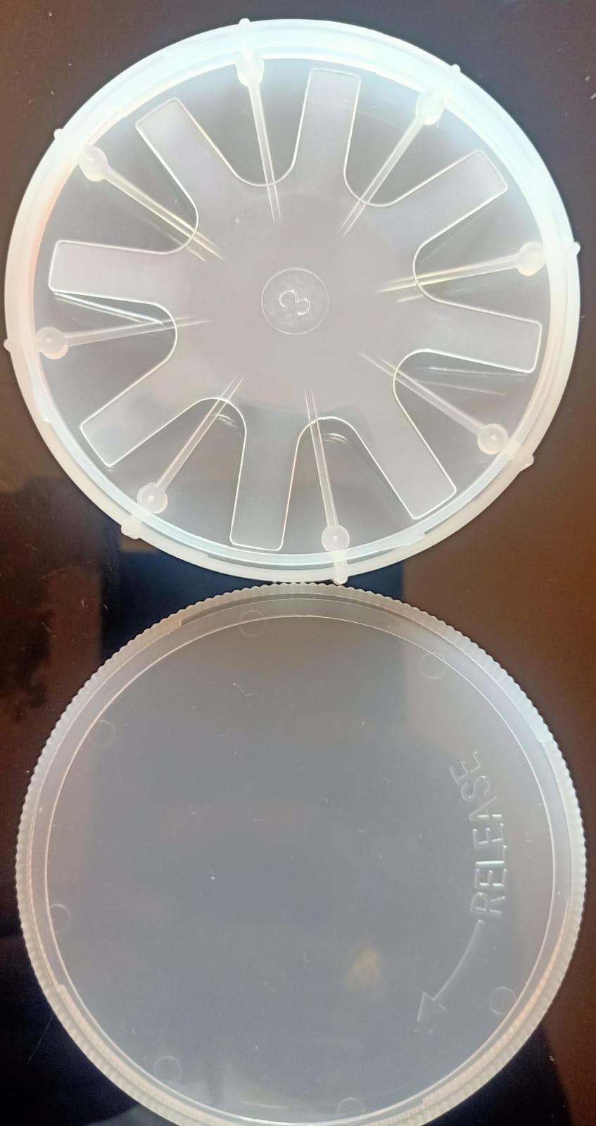
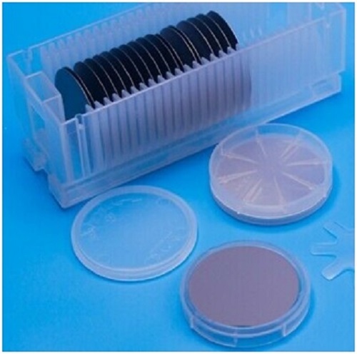
Silicon Wafer Carrier Box Polypropylene Material
Sizes Available:
- 4 inch
- 3 inch
- 2 inch
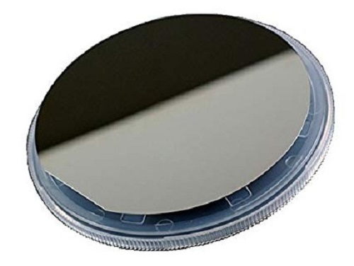
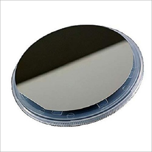
Silicon Wafer Carrier Box
Introduction
A silicon wafer carrier box is a specialized storage and transportation container designed to safely hold silicon wafers during handling, storage, and shipment. These carrier boxes play a critical role in the semiconductor industry by protecting delicate wafers from physical damage, contamination, electrostatic discharge (ESD), and environmental exposure.
Silicon wafers are extremely sensitive to scratches, particles, and mechanical stress. The wafer carrier box ensures that wafers remain clean, intact, and properly aligned throughout manufacturing, research, and logistics processes.
Purpose and Importance
The primary purpose of a silicon wafer carrier box is to maintain wafer integrity from fabrication to final use. During semiconductor processing, wafers pass through multiple steps and locations, making secure handling essential.
Wafer carrier boxes help to:
-
Prevent wafer breakage and chipping
-
Minimize particle contamination
-
Reduce handling-related defects
-
Ensure safe transportation between cleanroom environments
-
Maintain proper wafer orientation and spacing
These boxes are widely used in semiconductor fabs, research laboratories, universities, and wafer distribution facilities.
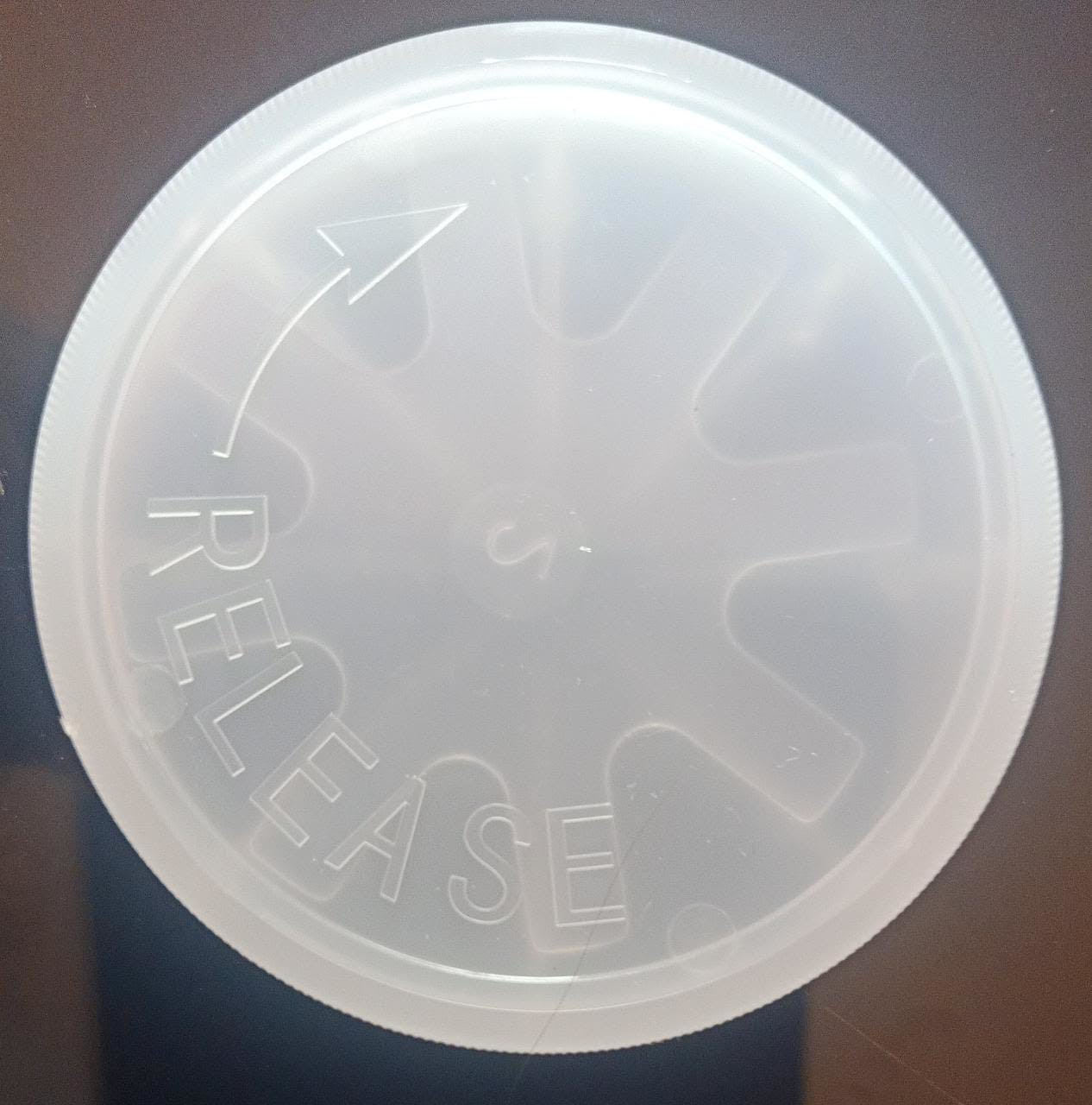
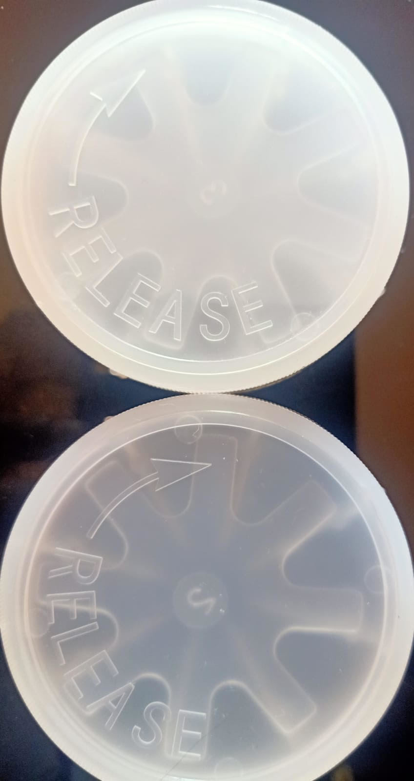
Material and Construction
Silicon wafer carrier boxes are typically manufactured from high-purity, cleanroom-compatible plastics. Common materials include polypropylene (PP), polycarbonate (PC), and antistatic or conductive polymers.
Key construction features include:
-
Lightweight yet rigid structure
-
Antistatic or ESD-safe material options
-
Smooth internal slots to prevent wafer scratching
-
Secure locking mechanism or snap-fit lid
-
Chemical resistance to cleaning agents
Some carrier boxes are designed for repeated use and can withstand cleanroom cleaning and sterilization processes.
Types of Silicon Wafer Carrier Boxes
1. By Wafer Size
Carrier boxes are available for standard wafer sizes such as 2-inch, 3-inch, 4-inch, 6-inch, 8-inch, and 12-inch. Each box is precisely designed to match wafer diameter and thickness.
2. By Capacity
Carrier boxes can hold different numbers of wafers, commonly ranging from 1 wafer to 25 wafers per box. Research labs often use low-capacity boxes, while industrial applications prefer higher-capacity carriers.
3. By Environment
Cleanroom-grade wafer carrier boxes are designed to meet ISO cleanroom standards, while general-purpose boxes are used for non-critical storage and transport.
4. By Protection Level
Some carrier boxes provide basic physical protection, while advanced designs include enhanced ESD protection and sealing against moisture and dust.
Applications
Silicon wafer carrier boxes are used across various stages of semiconductor and materials processing, including:
-
Wafer manufacturing and fabrication facilities
-
Semiconductor device assembly units
-
Research and development laboratories
-
University and academic research centers
-
Safe shipment of wafers to customers and partners
They are also used for handling other fragile substrates such as glass wafers, quartz wafers, and sapphire wafers.
Advantages of Silicon Wafer Carrier Boxes
-
Protect wafers from mechanical damage
-
Reduce contamination and particle exposure
-
Improve handling efficiency and safety
-
Reusable and cost-effective
-
Available in multiple sizes and configurations
These advantages make wafer carrier boxes an essential accessory in semiconductor and research environments.
Conclusion
Silicon wafer carrier boxes are a vital component in the safe handling, storage, and transportation of silicon wafers. By providing mechanical protection, contamination control, and ESD safety, they help maintain wafer quality and yield.
Whether used in advanced semiconductor fabrication plants or academic research laboratories, wafer carrier boxes ensure reliable wafer protection and contribute to efficient and defect-free operations.


Tell us about your requirement

Price:
Quantity
Select Unit
- 50
- 100
- 200
- 250
- 500
- 1000+
Additional detail
Mobile number
Email

More Products in Silicon Wafer Category

Silicon Wafer P Type : Diameter-2 inch
Price 2000 INR / Piece
Minimum Order Quantity : 1 Piece
Material : Single Crystal
Product Name : Silicon Wafer P Type : Diameter2 inch
Application : Semi conducted, Device, Solar, Substrate
Shape : Circular
2inch Silicon Wafer Intrinsic
Price 2000 INR / Piece
Minimum Order Quantity : 1 Piece
Material : Single Crystal
Product Name : Silicon Wafer Intrinsic : Diameter2 inch
Application : Semi conducted, Device, Solar, Substrate
Shape : Circular
4inch P Type Silicon Wafer
Price 3700.0 INR / Piece
Minimum Order Quantity : 1 Piece
Material : Single Crystal
Product Name : Silicon Wafer P Type: Diameter4 inch
Application : Semi conducted, Device, Solar, Substrate
Shape : Circular
Silicon Wafer Diameter Undoped : 4 inch
Price 3500.0 INR / Piece
Minimum Order Quantity : 1 Piece
Material : Single Crystal
Product Name : Silicon Wafer Diameter Undoped : 4 inch
Application : Semi conducted, Device, Solar, Substrate
Shape : Circular
Address
GST : 29AABCU9740P1ZH
- B- 205, Prime Blue Forest, Rajapallya, Hoodi,Bengaluru - 560048, Karnataka, India
- Phone :08071930855
- Send Inquiry
 |
ULTRANANOTECH PRIVATE LIMITED
All Rights Reserved.(Terms of Use) Developed and Managed by Infocom Network Private Limited. |
