|

 Send Inquiry
Hionic Planar Substrate - 5 x 5cm
Hionic Planar Substrate - 5 x 5cm Specification
- Hardness
- High
- Strength
- Excellent
- Purity
- 99.99%
- Product Type
- Planar substrate
- Material
- Ceramic substrate
- Shape
- Planar
- Moisture
- <0.05%
- Chemical Composition
- Customized composite oxides
- Application
- Microelectronics, sensor mounting, laser substrate
- Dimension (L*W*H)
- 5 x 5 cm
- Color
- White
- Electrical Insulation
- Excellent
- Thermal Conductivity
- High
- Surface Finish
- Polished
- Edge Quality
- Smooth cut edges
- Shelf Life
- 5 years
- Porosity
- Non-porous
- Temperature Stability
- Up to 1500°C
- Packaging
- Vacuum-sealed pouch
- Density
- 3.9 g/cm³
- Thickness Tolerance
- ±0.1 mm
Hionic Planar Substrate - 5 x 5cm Trade Information
- Payment Terms
- Paypal
- Delivery Time
- 15 Days
- Main Export Market(s)
- Asia
- Main Domestic Market
- All India
About Hionic Planar Substrate - 5 x 5cm
HionicPlanar Substrate - 5 x 5cm
Product Code: 6201619
Patentedscandia doped zirconia-based substrate for research on intermediate to hightemperature (700 - 900C) Solid Oxide Fuel Cell (SOFC) anode and cathodematerials. The Hionic substrate offers high strength for manufacturabilityalong with high conductivity for distinguishing subtle differences amongdifferent electrode materials.
TypicalUse Guidelines: Highly conductive Scandia based substrate for fabricatingsolid oxide fuel cells, or other high temperature applications. The Hionicsubstrates are ideal for long term testing, and other application whereimproved conductivity of an electrolyte support is desired.
Other Sizes AvailableInclude:
2.0 cm Diameter
2.5 cm Diameter
10 cm x 10 cm
Engineered for High-Performance Applications
This substrate is designed for demanding environments requiring durability and stability. Its advanced ceramic composition and polished finish make it ideal for precision applications in microelectronics, sensor integration, and optoelectronics. The non-porous structure and high purity ensure operational reliability and longevity.
Exceptional Material Properties
With superior thermal conductivity, outstanding electrical insulation, and resistance to extreme temperatures up to 1500C, this substrate offers versatile performance. Its dense, robust structure and fine surface finish make it suitable for both research and industrial uses, delivering consistent results even in rigorous conditions.
Secure Packaging and Longevity
Packed in a vacuum-sealed pouch, the substrate maintains its integrity during storage and transport. With a shelf life of five years and a moisture content below 0.05%, users benefit from minimized contamination risk and preserved quality, facilitating efficient inventory management for manufacturers and researchers alike.
FAQ's of Hionic Planar Substrate - 5 x 5cm:
Q: How is the Hionic Planar Substrate best used in electronic applications?
A: The Hionic Planar Substrate excels as a base for mounting microelectronic components, sensors, and lasers thanks to its high thermal conductivity, electrical insulation, and dimensional accuracy. Its robust and polished surface supports precise device integration and performance stability.Q: What specific benefits does its high thermal conductivity provide?
A: High thermal conductivity enables excellent heat dissipation, preventing overheating of sensitive components. This property enhances durability and reliability, especially in high-power or densely packed electronic assemblies.Q: When should I choose this substrate over alternatives?
A: Opt for this substrate when you need exceptional temperature resistance (up to 1500C), non-porosity, and superior electrical insulation. It is particularly suitable when device longevity and operational stability are critical requirements.Q: Where is the ideal environment to utilize this product?
A: The substrate is ideally used in controlled laboratory settings, clean rooms, and production lines for the microelectronics, optoelectronics, and sensor industries-anywhere high-purity and robust performance are essential.Q: What is the process for preparing the substrate for device mounting?
A: Prior to use, remove the vacuum-sealed substrate from its packaging in a clean environment. Its polished, smooth-edged surface requires minimal further treatment, streamlining your mounting or fabrication workflow.Q: How does packaging preserve substrate quality during storage and shipping?
A: Each substrate is vacuum-sealed to protect against moisture and contaminants, ensuring it maintains its 99.99% purity and structural integrity for up to five years in storage.Q: What advantages does this product offer over standard ceramic substrates?
A: This product stands out due to its precise dimension control, higher purity, superior temperature stability, and non-porous, dense structure, making it a preferred choice for cutting-edge microelectronic applications.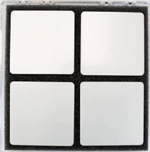
Tell us about your requirement

Price:
Quantity
Select Unit
- 50
- 100
- 200
- 250
- 500
- 1000+
Additional detail
Mobile number
Email

More Products in Solid Oxide Fuel Cell Components Category
Anode Supported Planar Cell - 5 x 5cm
Strength : Mechanical strength optimized for handling and sealing
Alloy : None (ceramic composite)
Application : Other, Fuel cell research, energy conversion, SOFC stack assembly
Dimension (L*W*H) : 5cm x 5cm x 0.15cm
Purity : 99.9% (main ceramic component)
Chemical Composition : NiOYSZ/YSZ/LSM or LSCF layered structure
Yttria-Stabilized Zirconia (8 mole %) a Nanopowder
Strength : High fracture toughness
Alloy : No alloy; Ceramic compound
Application : Other, Thermal barrier coatings, Solid oxide fuel cells, Dental ceramics, Oxygen sensors
Dimension (L*W*H) : Nanosized powder (average particle size: ~3060 nm)
Purity : 99.99%
Chemical Composition : ZrO : 9192%; YO : 8 mole%
Lanthanum Strontium Cobalt Ferrite Ink (LSCF6428)
Strength : Not applicable (liquid ink)
Alloy : No
Application : Other, SOFC cathodes, sensors, electronic ceramics, fuel cell devices
Dimension (L*W*H) : Custom packaging or bottle size; available in 10g, 25g, 100g
Purity : 99% (typical)
Chemical Composition : La0.6Sr0.4Co0.2Fe0.8O3 (Lanthanum Strontium Cobalt Ferrite)
Lanthanum Strontium Gallium Magnesium Oxide Powder
Strength : High mechanical strength
Alloy : No (ceramic oxide)
Application : Other, Solid Oxide Fuel Cells (SOFC), Ionic Conductors, Oxygen Sensors, Research & Development
Dimension (L*W*H) : Particle size: 15 micron (as powder)
Purity : 99.9% (trace metals basis)
Chemical Composition : La0.8Sr0.2Ga0.8Mg0.2O3
Address
GST : 29AABCU9740P1ZH
- B- 205, Prime Blue Forest, Rajapallya, Hoodi,Bengaluru - 560048, Karnataka, India
- Phone :08071930855
- Send Inquiry
 |
ULTRANANOTECH PRIVATE LIMITED
All Rights Reserved.(Terms of Use) Developed and Managed by Infocom Network Private Limited. |
