|

 Send Inquiry
Sputtering Target
Price 35000 INR/ Piece
MOQ : 1 , , Piece
Sputtering Target Specification
- Purity(%)
- 99.99%
- Usage & Applications
- Thin film deposition, semiconductor industry, magnetic data storage, optical coatings, solar cells
- Melting Point
- Depends on material; ultrahigh purity typically > 1000C
- Particle Size
- Sub-micron to micron-sized, customizable as per requirement
- Metal Type
- Transition, precious, or specialty metals, as specified
- Grade
- High Purity
- Boiling point
- Depends on material; generally > 2000C
- Product Type
- Metal Products
- Material
- Other
- Shape
- Round
- Chemical Composition
- 99.99% pure
- Density
- 11.3 Gram per cubic centimeter(g/cm3)
- Size
- Any diameter
- Weight
- Custom depending on target size and thickness
- Dimension (L*W*H)
- Custom, available as per customer specifications
- Color
- Metallic silver-grey
- Packaging
- Vacuum-sealed, cleanroom compatible
- Electrical Resistivity
- As per target material
- Thermal Conductivity
- Material specific, typically high
- Shape Options
- Round, planar, rotary, or custom-shaped
- Bonding Service
- Optional indium bonding for improved thermal conductivity
- Backing Plate
- Available upon request (Copper, Molybdenum, etc.)
- Sputtering Target Thickness
- 1 mm to 8 mm or as required
- Surface Finish
- Mirror polished, Ra < 0.3 m
Sputtering Target Trade Information
- Minimum Order Quantity
- 1 , , Piece
- Supply Ability
- 20 Pieces Per Month
- Delivery Time
- 15-25 Days
- Main Export Market(s)
- Eastern Europe, Middle East, Asia
- Main Domestic Market
- All India
About Sputtering Target
Features:
- From standard, single element materials to custom compounds, small circular to Multiple Tile and stepped constructions, and commercial grade to ultra-high purities
- We utilize a variety of specialized processing techniques such as hot pressing, hot isostatic pressing (HIP), and cold isostatic pressing (CIP), induction vacuum melting, and vacuum casting to produce homogenous, fine-grained, high-density materials that conform to the strictest application standards
- Provides a full range of sputtering target materials including precious metals, pure metals, alloys, ceramics, cermet, boride, oxides, carbides, nitrides, silicates, and fluorides
- Purities range from commercial-grade (99.5%) to ultra-high (99.9999%)
- Backing plates used in the sputtering process are essential to creating a quality thin film deposition for your product. We offer to backplates in both standard configurations and custom dimensions to meet your specific requirements. We also offer complete bonding services to provide a complete solution
1. Pure Metal Sputtering Target
Al, Sb, Bi, B, CD, C, Ce, Cr, Co, Cu, Dy, Er, Eu, Gd, Ge, Au, C, Hf, Ho, In, Ir, Fe, La, Lu, Mg, Mn, Mo, Nd, Ni, Nb, Pd, Pt, Pr,Re, Ru, Sm, Se, Sc, Ag, SI, Ta, Tb, Tm, Sn, Ti, W, V, Yb, Y, Zr, Zn, La, Ce, Pr, Nd, Sm, Eu, Gd, Tb, Dy, Ho, Er, Tm, Yb, Lu, Sc,Y
2. Alloy Sputtering Target
AlCu, AlCr, AlMg, AlSi, AlSiCu, AlAg, AlV, CaNiCrFe, CaNiCrFeMoMn, CeGd, CeSm, CrSi, CoCr, CoCrMo, CoFe, CoFeB, CoNi, CoNiCr, CoPt, CoNbZr, CoTaZr, CoZr, CrV, CrB, CrSi, CrCu, CuCo, CuGa, CuIn, CuNi, CoNiPt, CuZr, DyFe,DyFeCo, FeB, FeC, FeMn, GdFe, GdFeCo, HfFe, IrMn, IrRe, InSn, MoSi, NiAl, NiCr, NiCrSi, NdDyFeCo, NiFe, NiMn, NiNbTi,NiTi, NiV, SmCo, AgCu, AgSn, TaAl, TbDyFe, TbFe, TbFeCo, TbGdFeCo, TiAl, TiNi, TiCr, WRe, WTi, WCu, ZrAl, ZrCu, ZrFe,ZrNb, ZrNi, ZrTi, ZrY, ZnAl, ZnMg
3. Oxide sputtering Target or ceramic target
Al2O3, Sb2O3, ATO, BaTiO3, Bi2O3, CeO2, CuO, Cr2O3, Dy2O3, Er2O3, Eu2O3, Gd2O3, Ga2O3, GeO2, HfO2,Ho2O3, In2O3, ITO, Fe2O3, Fe3O4, La2O3, PbTiO3, PbZrO3, LiNbO3, Lu3Fe5O12, Lu2O3, MgO, MoO3, Nd2O3, Pr6O11, Pr,(TiO2) 2, Pr2O3, Sm2O3, Sc2O3, SiO2, SiO, SrTiO3, SrZrO3, Ta2O5, Tb4O7, TeO2, ThO2, Tm2O3, TiO2, TiO, Ti3O5, Ti2O3, SnO2, SnO, WO3, V2O5, YAG, Y3Al5O12, Yb2O3, Y2O3, ZnO, ZnO: Al, ZrO2 (unstabilized) , ZrO2-5-15wt% CaO)
4. Metal boride sputtering Target:
Cr2B, CrB, CrB2, Cr5B3, FeB, HfB2, LaB6, Mo2B, Mo2B5, NbB, NbB2, TaB, TaB2, TiB2, W2B, WB, VB, VB2, ZrB2
5. Metal Carbide Sputtering Target:
B4C, Cr3C2, HfC, Mo2C, NbC, SiC, TaC, TiC, WC, W2C, VC, ZrC
6. Fluoride sputtering Target
AlF3, BaF3, CdF2, CaF2, CeF3, DyF3, ErF3, HfF4, KF, LaF3, PbF2, LiF, PrF3, MgF2, NdF3, ReF3, SmF3, NaF, Cryolite, Na3AlF6, SrF2, ThF4, YF3, YbF3
7. Nitride Sputtering Target
AlN, BN, GaN, HfN, NbN, Si3N4, TaN, TiN, VN, ZrN
8. Selenide sputtering Target
Bi2Se3, CdSe, In2Se3, PbSe, MoSe2, NbSe2, TaSe2, WSe2, ZnSe
9. Silicide Sputtering Target
Cr3Si, CrSi2, CoSi2, HfSi2, MoSi2, NbSi2, TaSi2, Ta5Si3, TiSi2, Ti5Si3, WSi2, V3Si, VSi2, ZrSi2
Superior Material Purity & Customization
Our sputtering targets are manufactured from ultra-high purity materials (99.99%), ensuring reliable performance for critical thin film applications. With customizable thickness (1 mm to 8 mm or as specified) and shapes, we accommodate precise customer requirements for semiconductor, solar cell, and data storage technologies.
Flexible Backing Plate Solutions
Choose from copper, molybdenum, or other specialized backing plates to enhance target stability and heat dispersion. Indium bonding service is available by request for improved thermal conductivity during sputtering processes. Each backing plate is fitted to match your custom requirements.
Cleanroom Packaging & Quality Assurance
Each sputtering target is vacuum-sealed and prepared in cleanroom-compatible packaging to prevent contamination and preserve material integrity. Our rigorous quality standards ensure consistent mirror-polished finishes and high density, making them perfect for high-tech industries across India and worldwide.
FAQs of Sputtering Target:
Q: How is the sputtering target customized to my application requirements?
A: We offer full customization of sputtering target dimensions, shapes (round, planar, rotary, or custom), thickness (1 mm to 8 mm or as required), and particle size (sub-micron to micron). Chemical composition and grade can also be tailored to ensure suitability for your specific thin film deposition processes.Q: What backing plate and bonding options are available with your sputtering targets?
A: Backing plates made from copper, molybdenum, or other metals are available upon request. For improved thermal conductivity, optional indium bonding is offered to enhance the efficiency and reliability of the sputtering process.Q: When should I choose a mirror-polished surface finish for my sputtering target?
A: Opting for a mirror-polished surface (Ra < 0.3 m) is recommended when exceptionally smooth films and minimal surface contamination are required, particularly for critical semiconductor, optical, or magnetic coating applications.Q: Where is your sputtering target packaging performed, and is it suitable for cleanroom environments?
A: Our sputtering targets are vacuum-sealed and packaged in facilities designed to meet cleanroom standards. This process ensures product integrity and cleanliness, making them ideal for use in sensitive electronic, optical, and research environments.Q: What is the process for ordering a custom sputtering target and what details do I need to provide?
A: To order a custom sputtering target, share your required thickness, diameter, shape, backing plate material, purity level, particle size, and bonding preferences. Our technical team will guide you through the selection and manufacturing process for optimal results.Q: What are the main usage benefits of your sputtering targets for thin film deposition?
A: Our sputtering targets deliver consistent high purity, customizable dimensions, enhanced thermal conductivity, and versatile shapes. These features translate to superior film quality, minimal contamination, and adaptability for various industries including semiconductors, optics, data storage, and solar technology.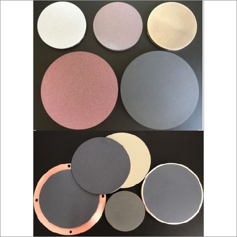
Tell us about your requirement

Price:
Quantity
Select Unit
- 50
- 100
- 200
- 250
- 500
- 1000+
Additional detail
Mobile number
Email

Address
GST : 29AABCU9740P1ZH
- B- 205, Prime Blue Forest, Rajapallya, Hoodi,Bengaluru - 560048, Karnataka, India
- Phone :08071930855
- Send Inquiry
 |
ULTRANANOTECH PRIVATE LIMITED
All Rights Reserved.(Terms of Use) Developed and Managed by Infocom Network Private Limited. |
