|

 Send Inquiry
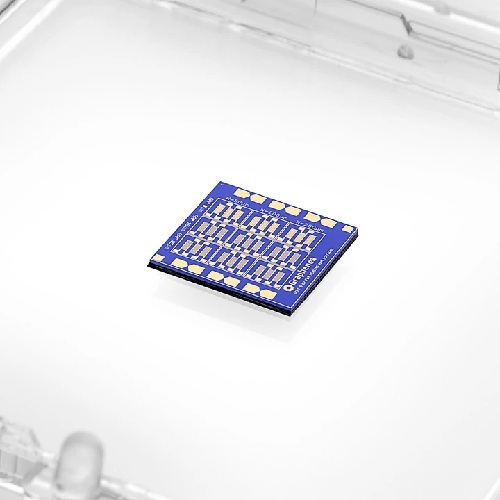
GFET-S12 for Sensing applications
Price 8000 INR/ Number
MOQ : 01 , , Number
GFET-S12 for Sensing applications Specification
- Measuring Range
- Highly sensitive, varies with analyte; typical detection limits in nM to pM range
- Power
- Low power consumption, <10 mW
- Usage & Applications
- Sensing applications including chemical, biological, and environmental analyte detection
- Display
- Not Applicable (output via signal measurement device)
- Interface
- 2-terminal/4-terminal with connectable electrodes
- Weight
- Approx. 3.2 g
- Size
- 12 mm x 12 mm
- Frequency
- DC to 100 kHz
- Material
- Graphene Field Effect Transistor (GFET)
- Temperature
- Operating Range: -10C to +85C
- Driven Type
- Electric field
- Voltage
- 0 to 2 V (Recommended Gate/Drain voltage)
- Storage Condition
- Store at room temperature, away from direct sunlight
- Response Time
- <1 second for most analytes
- Humidity Range
- 20% to 85% RH non-condensing
- Substrate
- Si/SiO wafer
- Channel Material
- Monolayer or few-layer graphene
- Contact Material
- Gold or Platinum
- Terminals
- Source, Drain, Gate pads with easy probe access
- Mobility
- >1500 cm/Vs (typical for monolayer graphene)
- Encapsulation
- Optional microfluidic chip compatible
GFET-S12 for Sensing applications Trade Information
- Minimum Order Quantity
- 01 , , Number
- Supply Ability
- 5 Per Day
- Delivery Time
- 25 Days
- Packaging Details
- seal pack
- Main Domestic Market
- All India
About GFET-S12 for Sensing applications
Discover the GFET-S12, a best-seller for unmatched sensing applications in India. This exceptional device features sought-after monolayer or few-layer graphene channels, optional microfluidic chip compatibility, and robust gold or platinum contacts. Buy online from distributor, manufacturer, supplier, retailer, or trader to access its magnificent sensitivity (nM to pM range) and swift response time (<1s). Enjoy reliable operation across 20-85% RH and -10C to +85C, with easy probe access and low power consumption (<10 mW). Secure your offer now for innovative chemical, biological, and environmental sensing.
Versatile Usage and Standout Features of GFET-S12
GFET-S12 is widely used for chemical, biological, and environmental sensing applications, offering highly sensitive detection down to nanomolar or picomolar levels. Key features include monolayer graphene for superb mobility (>1500 cm2/Vs), optional encapsulation for added flexibility, rapid response time under 1 second, and easy terminal access. The device operates efficiently from -10C to +85C, consumes less than 10 mW power, and supports 2-terminal or 4-terminal configurations, making it a reliable solution for advanced sensing needs.
Swift Delivery and Main Domestic Market Advantages
GFET-S12 units are typically handed over to customers within a prompt delivery time to ensure quick project initiation. The main domestic market is India, with comprehensive support from renowned distributors and suppliers. Sample units are available for valuation, allowing clients to assess performance before the proposal amount is finalized. Flexible purchase options and responsive customer service guarantee a smooth procurement experience for manufacturers, researchers, and traders throughout India.
FAQ's of GFET-S12 for Sensing applications:
Q: How can I buy the GFET-S12 for sensing applications?
A: You can buy the GFET-S12 online through authorized distributors, manufacturers, suppliers, or retailers in India. Reach out to listed traders for availability and purchasing options.Q: What makes the GFET-S12 exceptional compared to other sensing devices?
A: The GFET-S12 offers outstanding mobility, rapid response time, high sensitivity, and reliable operation over wide temperature and humidity ranges, making it highly sought-after for advanced sensing tasks.Q: Where can the GFET-S12 be used most effectively?
A: GFET-S12 is ideal for chemical, biological, and environmental analyte detection in laboratories, research institutions, and industrial monitoring settings.Q: What is the usual delivery process for GFET-S12 orders?
A: Orders are swiftly processed and handed over to clients, with sample units available for valuation before confirming the full proposal amount.Q: What benefits does the optional microfluidic chip compatibility provide?
A: Microfluidic compatibility allows for enhanced analyte manipulation, supporting more complex sensing protocols and experiments.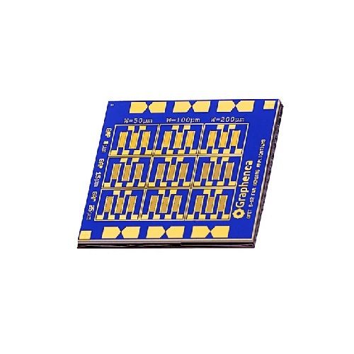
Tell us about your requirement

Price:
Quantity
Select Unit
- 50
- 100
- 200
- 250
- 500
- 1000+
Additional detail
Mobile number
Email

More Products in Sensing Applications Category

GFET-S10 for Sensing applications
Price 15000 INR / Number
Minimum Order Quantity : 01 , , Number
Size : 10 mm x 10 mm chip
Interface : 2pin terminal (source and drain contacts)
Measuring Range : Conductance modulation response up to 80 S
Weight : Approx. 2 g
GFET-S11 for Sensing applications
Price 8000 INR / Number
Minimum Order Quantity : 01 , , Number
Size : 11 mm 11 mm
Interface : Twoterminal and Fourterminal
Measuring Range : 1 pM to 1 mM (analyte dependent)
Weight : 3 grams
GFET-S20 for Sensing applications
Price 20000 INR / Number
Minimum Order Quantity : 01 Number, ,
Size : 20 mm x 20 mm
Interface : Electrical contacts (source, drain, gate)
Measuring Range : pico to micromolar concentration detection
Weight : Approx. 2 grams
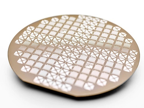
GFAB - Graphene Foundry Service
Price 10000 INR / Number
Minimum Order Quantity : 01 , , Number
Size : Custom wafers and substrates
Interface : Service includes design and integration
Measuring Range : Layer thickness from monolayer to multilayer
Weight : Depends on substrate and layers
Address
GST : 29AABCU9740P1ZH
- B- 205, Prime Blue Forest, Rajapallya, Hoodi,Bengaluru - 560048, Karnataka, India
- Phone :08071930855
- Send Inquiry
 |
ULTRANANOTECH PRIVATE LIMITED
All Rights Reserved.(Terms of Use) Developed and Managed by Infocom Network Private Limited. |
