|

 जांच भेजें
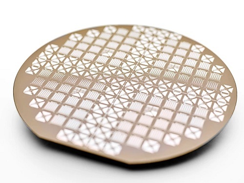
GFAB - ग्राफीन फाउंड्री सर्विस
Price 10000 आईएनआर/ Number
MOQ : 01 , , Number
GFAB - ग्राफीन फाउंड्री सर्विस उत्पाद की विशेषताएं
- अंतरफलक
- Service includes design and integration
- मटेरियल
- Graphene
- तापमान
- Process compatible up to 300°C
- वोल्टेज
- Process variable, depends on device requirements
- वज़न
- Depends on substrate and layers
- फ़्रिक्वेंसी
- Supports GHz range for RF applications
- चालित प्रकार
- Wafer-based fabrication
- साइज
- Custom wafers and substrates
- मापने की सीमा
- Layer thickness from monolayer to multilayer
- उपयोग/अनुप्रयोग
- Research, Electronics, Sensors, Photonics, RF Devices
- Substrate Options
- SiO2/Si, Sapphire, Flexible Polymers
- Customization
- Available for patterns, contacts, and device structure
- Production Capability
- Pilot to mass production
- Delivery Format
- As-fabricated wafers, patterned chips, or diced samples
- Service Support
- Technical consulting, process development
- Surface Preparation
- Ultra-clean, prepared for subsequent processing
- Layer Uniformity
- High uniformity across wafer
- Thickness Control
- Monolayer to few-layer (1–10 layers)
- Device Integration
- Compatible with MEMS, CMOS, and hybrid integration
- Purity
- 99.9% graphene
GFAB - ग्राफीन फाउंड्री सर्विस व्यापार सूचना
- Minimum Order Quantity
- 01 , , Number
- भुगतान की शर्तें
- पेपैल
- आपूर्ति की क्षमता
- 5 प्रति दिन
- डिलीवरी का समय
- 25 दिन
- पैकेजिंग का विवरण
- एक डिब्बे में सील पैक
- मुख्य घरेलू बाज़ार
- ऑल इंडिया


Tell us about your requirement

Price: Â
Quantity
Select Unit
- 50
- 100
- 200
- 250
- 500
- 1000+
Additional detail
मोबाइल number
Email

अधिक Products in संवेदन अनुप्रयोग Category

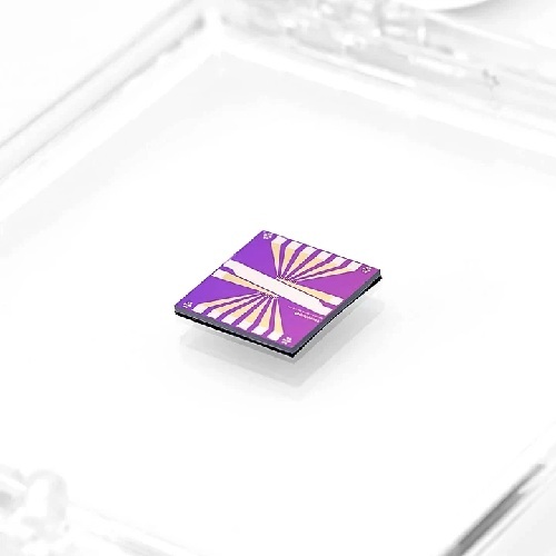
सेंसिंग अनुप्रयोगों के लिए GFET-S10
तापमान : Operating: 20°C to +60°C
मटेरियल : Graphene
उपयोग/अनुप्रयोग : Biosensing, gas sensing, chemical detection, environmental monitoring
अंतरफलक : 2pin terminal (source and drain contacts)
पावर : <0.5 W, low power consumption
मूल्य या मूल्य सीमा : आईएनआर
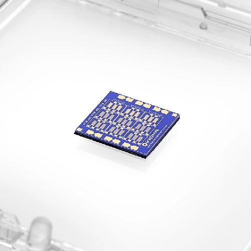
सेंसिंग अनुप्रयोगों के लिए GFET-S20
तापमान : 20°C to 60°C
मटेरियल : Highquality Graphene
उपयोग/अनुप्रयोग : Chemical and biological sensing
अंतरफलक : Electrical contacts (source, drain, gate)
पावर : Low power consumption (<0.1 W)
मूल्य या मूल्य सीमा : आईएनआर
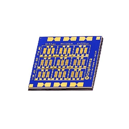
सेंसिंग अनुप्रयोगों के लिए GFET-S11
तापमान : 40°C to +85°C
मटेरियल : Graphene
उपयोग/अनुप्रयोग : Biosensing, Chemical Sensing, Detection of Gases and Biomolecules
अंतरफलक : Twoterminal and Fourterminal
पावर : <50 mW
मूल्य या मूल्य सीमा : आईएनआर
सेंसिंग अनुप्रयोगों के लिए GFET-S12
तापमान : Operating Range: 10°C to +85°C
मटेरियल : Graphene Field Effect Transistor (GFET)
उपयोग/अनुप्रयोग : Sensing applications including chemical, biological, and environmental analyte detection
अंतरफलक : 2terminal/4terminal with connectable electrodes
पावर : Low power consumption, <10 mW
मूल्य या मूल्य सीमा : आईएनआर
Address
GST : 29AABCU9740P1ZH
- बी-205, प्राइम ब्लू फॉरेस्ट, राजपाल्या, हुडी,बैंगलोर - 560048, कर्नाटक, भारत
- फ़ोन :08071930855
- जांच भेजें
 |
ULTRANANOTECH PRIVATE LIMITED
सर्वाधिकार सुरक्षित.(उपयोग की शर्तें) इन्फोकॉम नेटवर्क प्राइवेट लिमिटेड . द्वारा विकसित एवं प्रबंधित |
