|

 जांच भेजें
सà¥à¤à¤¸à¤¿à¤à¤ ठनà¥à¤ªà¥à¤°à¤¯à¥à¤à¥à¤ à¤à¥ लिठGFET-S10
Price 15000 आईएनआर/ Number
MOQ : 01 , , Number
सà¥à¤à¤¸à¤¿à¤à¤ ठनà¥à¤ªà¥à¤°à¤¯à¥à¤à¥à¤ à¤à¥ लिठGFET-S10 Specification
- मापने की सीमा
- Conductance modulation response up to 80 μS
- तापमान
- Operating: -20°C to +60°C
- साइज
- 10 mm x 10 mm chip
- वोल्टेज
- Drain Voltage (Vds): 0-1 V; Gate Voltage (Vg): -2 V to +2 V
- फ़्रिक्वेंसी
- DC to 1 KHz
- उपयोग/अनुप्रयोग
- Biosensing, gas sensing, chemical detection, environmental monitoring
- वज़न
- Approx. 2 g
- चालित प्रकार
- Electrical (voltage controlled)
- अंतरफलक
- 2-pin terminal (source and drain contacts)
- मटेरियल
- Graphene
- पावर
- <0.5 W, low power consumption
- डिसप्ले
- No onboard display
सà¥à¤à¤¸à¤¿à¤à¤ ठनà¥à¤ªà¥à¤°à¤¯à¥à¤à¥à¤ à¤à¥ लिठGFET-S10 Trade Information
- Minimum Order Quantity
- 01 , , Number
- भुगतान की शर्तें
- पेपैल
- आपूर्ति की क्षमता
- 5 प्रति दिन
- डिलीवरी का समय
- 25 दिन
- पैकेजिंग का विवरण
- एक डिब्बे में पैक बंद कर दें
- मुख्य निर्यात बाजार
- एशिया
- मुख्य घरेलू बाज़ार
- ऑल इंडिया
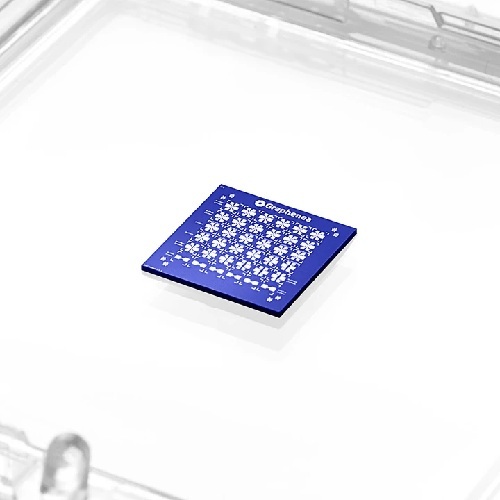
About सà¥à¤à¤¸à¤¿à¤à¤ ठनà¥à¤ªà¥à¤°à¤¯à¥à¤à¥à¤ à¤à¥ लिठGFET-S10
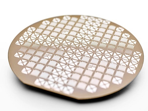
Discover the reduced advance purchase opportunity and get the unassailable GFET-S10 graphene sensor chip now. Featuring CVD-grown monolayer graphene as the channel material and gold electrodes on a silicon/silicon dioxide substrate, this wondrous 10 mm x 10 mm chip offers ravishing carrier mobility above 1000 cm2/Vs. Unencapsulated, it allows direct analyte exposure-perfect for biosensing and environmental monitoring. Packaged in an ESD-safe, vacuum-sealed box, it ensures safety and compliance. Optional customization with microfluidics and microelectrodes elevates sensing precision. Available for distributor, manufacturer, supplier, retailer, and trader partners across India.
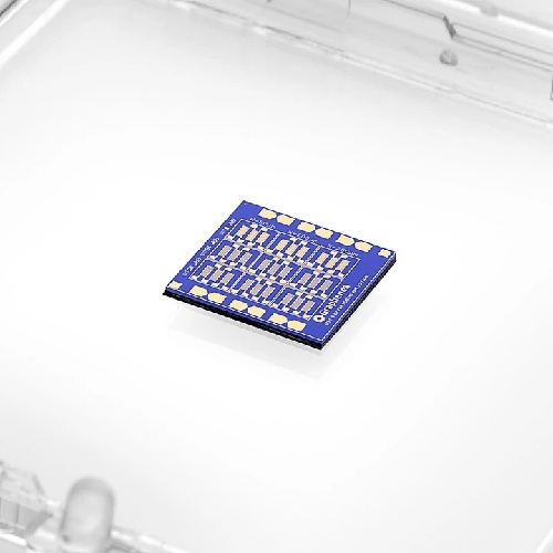
GFET-S10 Sensing Applications: Usage, Features, and Directions
GFET-S10, designed for advanced sensing applications like biosensing and gas detection, offers an open, unencapsulated surface for direct analyte exposure. Use the 2-pin terminal interface, applying controlled voltages for conductance modulation. Its key features include high carrier mobility, low contact resistance, and low power requirements, making it ideal for precision measurements. Customization for microfluidics or microelectrodes is available, enhancing its wonderous versatility and performance in laboratory or research environments.
Serving Markets & Transactions: GFET-S10 Distribution
The GFET-S10 caters to the main domestic market of India and is also shipped to select export markets globally. Order processing is efficiently managed, ensuring fast turnaround until goods are handed over to reliable shippers. Accepted payment terms include advance payment and institutional purchase orders, streamlining transactions for manufacturers, suppliers, retailers, distributors, and traders. Every box is meticulously vacuum-sealed and ESD-protected, ready for timely dispatch and global delivery.
FAQ's of GFET-S10 for Sensing applications:
Q: How is the GFET-S10 used in sensing applications?
A: The GFET-S10 is typically integrated into sensing setups where its open graphene surface directly interacts with target analytes. It operates by applying voltage to the source and drain contacts, allowing researchers to observe conductance changes for biosensing, chemical detection, or environmental monitoring.Q: What are the main features that make GFET-S10 unassailable for detection tasks?
A: Its CVD-grown monolayer graphene ensures high sensitivity, while gold electrodes offer excellent conductivity. With a reduced contact resistance and high carrier mobility, the chip delivers ravishing performance in a compact 10 mm x 10 mm form, ideal for demanding sensing environments.Q: When should custom microfluidics or microelectrode integration be considered?
A: Customization should be requested during the order process if your application requires enhanced specificity or additional functional interfaces, such as microfluidic channels for biochemical analysis or extra electrodes for multiplexed sensing.Q: Where is GFET-S10 mainly distributed and shipped?
A: The GFET-S10 is primarily distributed within India, serving the domestic market. However, it is also available for export to select international markets through authorized distributors, ensuring global reach.Q: What is the process for ordering and receiving the GFET-S10?
A: Orders are initiated by contacting a local distributor, manufacturer, or supplier. Once processed and payment terms are settled, the product is vacuum-sealed, ESD-protected, and shipped promptly. Handover to logistical partners ensures safe delivery to your location.Q: What benefits does direct analyte exposure provide for users?
A: The unencapsulated, open graphene surface allows direct interaction with analytes, which maximizes sensitivity and response accuracy. This design feature supports ravishingly precise biosensing, gas detection, and real-time chemical analysis.
Tell us about your requirement

Price: Â
Quantity
Select Unit
- 50
- 100
- 200
- 250
- 500
- 1000+
Additional detail
मोबाइल number
Email

अधिक Products in संवेदन अनुप्रयोग Category
सेंसिंग अनुप्रयोगों के लिए GFET-S11
मूल्य या मूल्य सीमा : आईएनआर
मटेरियल : Graphene
तापमान : 40°C to +85°C
माप की इकाई : , , नंबर
मूल्य की इकाई : नंबर
चालित प्रकार : Electronic
सेंसिंग अनुप्रयोगों के लिए GFET-S20
मूल्य या मूल्य सीमा : आईएनआर
मटेरियल : Highquality Graphene
तापमान : 20°C to 60°C
माप की इकाई : नंबर, ,
मूल्य की इकाई : नंबर
चालित प्रकार : Externally powered
सेंसिंग अनुप्रयोगों के लिए GFET-S12
मूल्य या मूल्य सीमा : आईएनआर
मटेरियल : Graphene Field Effect Transistor (GFET)
तापमान : Operating Range: 10°C to +85°C
माप की इकाई : , , नंबर
मूल्य की इकाई : नंबर
चालित प्रकार : Electric field
GFAB - ग्राफीन फाउंड्री सर्विस
मूल्य या मूल्य सीमा : आईएनआर
मटेरियल : Graphene
तापमान : Process compatible up to 300°C
माप की इकाई : , , नंबर
मूल्य की इकाई : नंबर
चालित प्रकार : Waferbased fabrication
Address
GST : 29AABCU9740P1ZH
- बी-205, प्राइम ब्लू फॉरेस्ट, राजपाल्या, हुडी,बैंगलोर - 560048, कर्नाटक, भारत
- फ़ोन :08071930855
- जांच भेजें
 |
ULTRANANOTECH PRIVATE LIMITED
सर्वाधिकार सुरक्षित.(उपयोग की शर्तें) इन्फोकॉम नेटवर्क प्राइवेट लिमिटेड . द्वारा विकसित एवं प्रबंधित |
